Custom Electron Columns
We design and build the electron column at the heart of your instrument — from first principles to production-ready hardware. You keep the instrument. We deliver the column.

The column is the hard part. You don't have to build it yourself.
The electron column — source, optics, beam control — is the hardest and most valuable subsystem in any electron-beam instrument. Almost every manufacturer designs and builds it in-house, behind closed doors, at the cost of a dedicated team and years of iteration.
We are the independent alternative. BeamShape designs columns from first principles, proves them in simulation, and builds them in metal — so you can bring an advanced instrument to market without building an electron-optics group from scratch.
In-house example: A 60 kV, 2 kW electron-beam column that sees what it does
Anyone can show a simulation. Far fewer can show the metal that matches it.

Our flagship, built in-house under our EBMelt program, is a 60 kV, 2 kW electron-beam column for electron-beam melting and welding — with an integrated backscatter (BSE) detector that brings SEM-like navigation and metrology to the process itself.
Most electron-beam melting and welding is blind: the beam does its work and you find out afterwards whether it went right. This column doesn't just deliver the beam — it lets you see and measure what the beam is doing, live, in vacuum. That is the demonstration that our columns span the full range, from melting-level power to imaging resolution, and that our simulations hold up in hardware.
60 kV · 2 kW · integrated BSE imaging · electron-beam melting + welding · in-vacuum navigation and metrology
What we build
We develop complete columns and individual subsystems, across the full range of charged-particle optics.
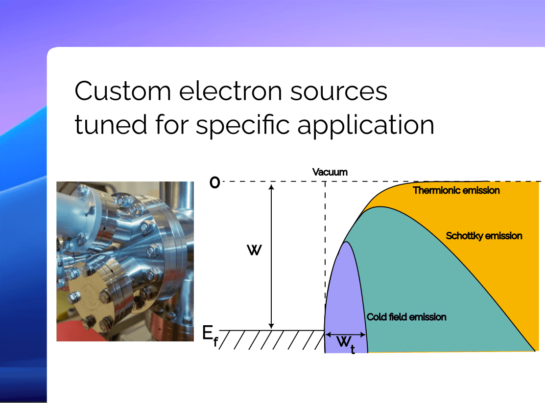
Electron sources for applications in microscopy, defect analysis, X-ray generation and high power applications.
Create with us very stable electron sources from low voltage to high voltage applications.
We can help you with all the conventional electron emitter designs for different vacuum uses and different beam powers.
We are able to design, manufacture, test and ship finalized systems to our OEM partners.
Emitters are being assembled and tested in clean rooms in our facility in Brno, Czech Republic.
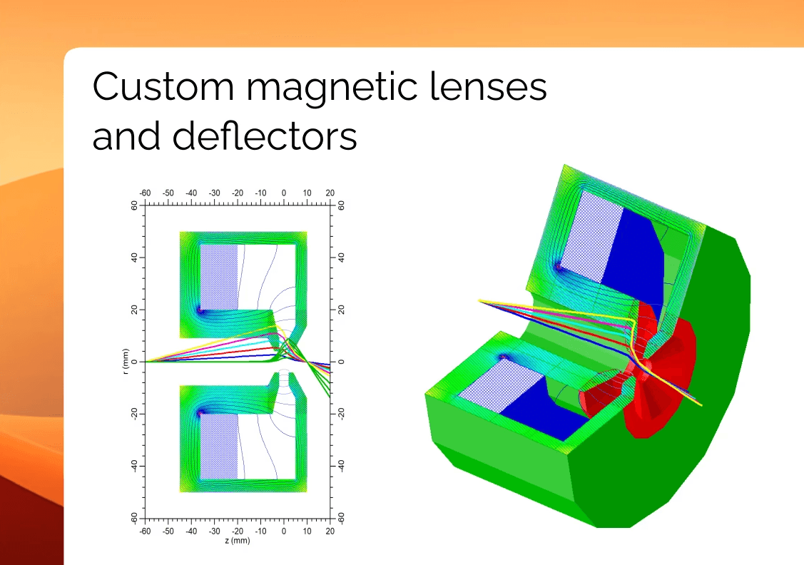
Every application-specific electron system needs also custom-designed electron optics. There is no place for generalist design in targeted applications.
We are able to design mangetic lenses and complex deflection system. Our network of trusted suppliers for machining of magnetic materials allows us to manufacture such solutions in record time.
Modules are tested by us before shipping to our OEM partners.

From scintillation-based detectors and semiconductor diodes to Medipix-based electron cameras tuned to your specifications.
We have suppliers of key elements of the detectors and we build around our solution to fit into strict OEM requirements.
We have long experience in this industry and we know the struggles with building complex electron beam systems.
We are prepared to take responsibility for design, manufacturing and testing of larger electron beam systems based on your specifications.
Brno, Czech Republic is the center of electron microscopy industry in the world and we are leveraging the local suppliers heavily to bring the most advanced electron beam products.
Collaboration is typically done under strict NDA with only small team involved. Assembly and testing of systems are done in clean rooms and laboratories with limited access.
Support